When assembling complex electronic products, engineers often need to join small daughter cards with large motherboards. Press-fit connectors and ball grid array (BGA) connectors have recently been introduced to make this task easier and less costly. These connectors can transfer large amounts of data at high speeds. They also perform better electrically than through-hole connectors.
Contract manufacturers prefer BGA connectors because they do not require wave soldering. They are placed on the board and soldered during reflow like any other surface mount component. And, like all area array components, BGA connectors have the inherent ability to self-center during reflow.
Unfortunately, little data exists on the ideal parameters for assembling these connectors or on their long-term reliability. We conducted a study to find out.
Our study looked at five different connectors:
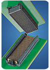
- Backplane A-a press-fit connector with 192 I/O, measuring 1.8 by 1.35 millimeters.
- Backplane B-a press-fit connector with 120 I/O, measuring 2.5 by 1.5 millimeters.
- Mezzanine A-a BGA connector with 666 I/O, measuring 1 by 1.3 millimeters.
- Mezzanine B-a BGA connector with 300 I/O, measuring 1.27 by 1.27 millimeters.
- Socket-a BGA connector with 700 I/O, measuring 1.27 by 1.27 millimeters.
Our test board, dubbed "Metropolis," contained two samples of each connector. The connectors were spaced far enough apart to ensure even heating during reflow and adequate air circulation during accelerated thermal cycling (ATC) tests.
Besides the components themselves, we looked at the impact of surface finish on connector reliability. We studied three finishes: organic solder preservative (OSP); electroless nickel, immersion gold (ENIG); and immersion silver. We also assessed the effects of rework on reliability.
When designing Metropolis, we followed the guidelines in IPC-9701, which governs reliability testing of surface mount components. Although this standard was not written with BGA connectors in mind, it was a useful starting point.
One difference from the standard was in the implementation of daisy chains through the components. When building test boards for BGAs, a daisy-chained version of the package must be obtained from the supplier. These packages are then mounted on a test board that is designed to connect the daisy-chain links inside the package to form a continuous loop through the board and component.
For our study, daisy-chained versions of BGA connectors were not available, so actual production parts were used. The daisy chain was created entirely within the test board. For example, to evaluate a mezzanine connector, two circuit boards were used-one for the motherboard and one for the daughter card. Once the test boards were assembled, a complete daisy chain circuit through the connector and the two PCBs was created, which allowed resistance measurements to be made during ATC. To test the socket, daisy-chained dummy processors were used.
We added several features to the test board to facilitate reliability testing. Test points were used to subdivide the daisy chains into shorter subsections. This helped to isolate electrical failures during ATC. The ability to jump past failed components allowed more than one component to be placed on a single daisy chain. As a result, fewer in-situ monitoring channels were needed, which reduced the cost of our study. The monitoring headers on the test board were surface mount pin headers, which allowed the test boards to be assembled without wave soldering.
A unique feature of our test board was the hardware for the socket assembly. With chamber space at a premium and pressure to keep project costs down, we decided to use a simple aluminum plate to mimic the complex and costly heat sink. Ordinarily, a large heat sink mounted on a metal frame is needed to dissipate the heat generated by the processor during operation. This frame is riveted to the board around the socket.
Unfortunately, the metal frame was too large for our test board. Rather than design a larger board, we cut the frame so that only the portion required for the test was left. The heat-dissipation function of the heat sink was not necessary for our tests. However, because the heat sink exerts a compression load on the processor, we could not do without it completely.
Assembling the Boards
For the BGA connectors, our primary objective was to collect reliability data through ATC tests. For the press-fit connectors, the primary goal was to measure insertion and retention forces for leads plated with tin-lead and those plated with pure tin.Performance in ATC tests is a relative measure of reliability. Although ATC is typically used to accelerate fatigue failure of solder joints, it is a relevant test for press-fit joints, too. There are many failure modes for press-fit contacts, but fretting corrosion is one that may be accelerated by thermal cycling. Temperature changes can cause micro motion at the contact interface. This causes wear in the joint, which can eventually lead to detectable increases in contact resistance. These data can provide a sense of the relative performance of the connectors with different surface finishes. It can also be used to compare the performance of the tin-lead plated connectors with that of the lead-free connectors.
The motherboards and daughter cards were printed with standard tin-lead solder paste.
A fine-pitch placement machine positioned all the connectors. Mezzanine connector B was easily picked from a tape-and-reel and placed using standard nozzles. The socket, which was packaged in JEDEC trays, was also picked using standard nozzles. Mezzanine connector A was packaged in thermoformed plastic trays, so vibratory feeders were used to feed it. Two different sizes of mezzanine connector A were included in the study. On the motherboard, we used receptacles that were 5 millimeters tall and 15 millimeters tall. On the daughter card, we used plugs that were 10 millimeters tall and 20 millimeters tall. We experienced no difficulties with either size.
All the boards were reflowed in a 10-zone convection oven with a nitrogen atmosphere.
A set of reworked samples was included in the test plan. Ten sites per connector type on each surface finish were selected for rework. Only the taller versions of mezzanine connector A were reworked. Given the height and internal construction of the taller version, we suspected that it would be more prone to reliability issues. Reworked samples were also included in the ATC testing.
Following reflow, the press-fit connectors were installed in the daughter cards and the motherboard, and the insertion force was measured. Then, ten connectors of each type were removed and replaced, and the insertion force of the second placement was measured.
Finally, the daughter cards were mated to the motherboards, and hardware, such as standoffs and heat sinks, were added. The assemblies were then ready for ATC.
Testing the Boards
The assemblies were divided into two thermal cycling chambers. The tin-lead assemblies were placed in one chamber; the lead-free press-fit assemblies were placed in the second.We followed the preferred thermal cycle profile outlined in IPC-9701. The temperature cycled from 0 C to 100 C. Test time was 90 minutes for the tin-lead assemblies, and 60 minutes for the lead-free press-fit assemblies. The mass and the complex geometry of the assemblies precluded the use of a faster profile.
During ATC, the assemblies were monitored in-situ using data loggers. A net was deemed to have failed when five consecutive readings showed a 20 percent or greater increase in resistance from the baseline measurement. The test was stopped periodically to isolate the damaged pins on the failed nets. The boards were designed to allow each connector to be cut out from the assembly without damaging the connections to the remaining connectors. This allowed us to conduct failure analysis as soon as possible after a failure was detected.
Thirty motherboards were assembled with a socket and heat sink assembly on the top side and just a socket on the opposite side. Only the topside socket was monitored during testing. Of those 30 boards, 15 underwent vibration testing, and 15 assemblies underwent torque testing. All 30 boards passed these tests with no increases in resistance.
Test Results
As expected, most of the failures found with mezzanine connector B were related to solder joint fatigue. We found little difference in reliability between the three surface finishes. The OSP finish appears to provide slightly better reliability, but the sample size was too small for us to conclude definitively that OSP is better than other finishes.For immersion silver, the reliability of newly assembled and reworked connectors is similar. However, for ENIG, the reworked connectors proved to be slightly less reliable than the newly assembled connectors. Among the reworked connectors, 1 percent of the sample population failed after less than 100 cycles. In contrast, it took more than 300 cycles for 1 percent of the newly assembled connectors to fail. This was unexpected, and we did additional analysis to determine the root cause.
As each component failed, the location of the failing pins was isolated using a multimeter. Selected components were then cut out from the test boards for further analysis. The procedure for removing a connector from the board was more complex than for BGAs, because the possibility of contact failures had to be taken into consideration.
First, the standoff hardware was removed, and the daughter card was carefully unmated from the motherboard. The contacts attached to each of the failed pins were examined for contamination or unusual wear. This was done to determine if the increase in resistance was due to a contact failure. The section of the motherboard containing the samples was then cut out. If no signs of damage to the contacts was detected, the samples were cross-sectioned to determine if the solder joints had failed. The unmated motherboard and daughter cards were trimmed and potted. Cross sections were made at the first failure locations, and the failure mode for each sample was determined.
The cross sections revealed that most samples failed on the daughter card. The cracks were found to be typical fatigue failures, though they formed on the board side of the joint rather than the component side. This is likely due to the unusual ball attachment method at the component side. The balls are not soldered to flat pads as they would be in a conventional BGA. Instead, they are reflowed onto pins that form part of the contacts. The cracks observed in the failed joints propagated through the bulk solder above the intermetallic layer on the board side.
In four cases, we found cracks on both the motherboard and the daughter card. In each case, we found similar fatigue cracks, all of which were on the board side of the joint.
As the failure locations were isolated, we noticed that the failures were occurring in a pattern. We plotted a map of the failure locations for each connector site and each surface finish. Our diagrams indicated that the failures were not limited to the distance from the neutral point, as was expected. Instead, the failures were concentrated along the length of the connectors, clustering near the middle of the long edge. Another unexpected observation was that the failures did not occur symmetrically on both long edges of the connector. Neither surface finish nor rework was a factor in failure location.
We investigated further to determine why the failures appeared where they did. Coefficient of thermal expansion (CTE) measurements had previously been made on a connector from the product family of mezzanine connector B. The connector had the same footprint as the receptacle we used in our test, but was slightly taller. Samples of the plastic housing material were removed, and the CTE was measured by digital speckle correlation. These measurements determined that the CTE of the connector was different in the X, Y and Z axes, due to variations in the flow of the polymer during molding.
We found that the CTE in the X axis, measured near the center of the connector, was approximately 15 ppm/C. This closely matches the motherboard's CTE of 13 to 14 ppm/C. However, in the Y direction, the CTE of the connector was higher, 23 to 27 ppm/C. Thus, in the Y direction, there was a CTE mismatch between the board and connector. This helps explain why failures formed along the long edges of the connector, but it does not fully explain why the failures were concentrated on the inside edges of the connector, or why they appeared primarily on the daughter card.
The CTE in the Z axis was relatively high-84 to 97 ppm/C. The CTE of stainless steel, the material used for the standoffs, is 10 to 17 ppm/C. Based on these numbers, we believe the system behaves like this: As the assembly heats up, the connectors expand in the Z axis. The standoffs also expand, though not as much due to their lower CTE. Because the daughter card is thinner and more compliant than the motherboard, it bows upward as the connectors expand, and a tensile stress is exerted on the card. Simultaneously, the daughter card, motherboard and connectors expand in the X and Y directions. On a solder joint level, this would indicate that the failures would occur primarily on the daughter card.
Because the CTE of the connector in the Y direction exceeds the CTE of the board, the connector will expand at a greater rate than the board. As a result, on the outside row of balls, closest to the standoff, the tensile stress in the card and the stress from the expansion of the connector act in the same direction, and the solder joint experiences a relatively lower strain. On the inner row, the tensile stress in the card and the stress from the expansion of the connector relative to the board act in opposite directions, resulting in a higher strain on the solder joint. As a result, the inner rows of balls would fail first.
Based on this theory, engineers should use standoffs of a material that more closely matches the CTE in the Z direction of the connectors. This may distribute the stresses on the joints more evenly and prolong fatigue life.
After 4,200 thermal cycles, there have been only two failures of the socket. The failures occurred at between 3,100 and 3,600 cycles. The failures were isolated to the peripheral row of joints located in the middle of the socket. Neither model of mezzanine connector A has experienced an electrical failure.
As for the press-fit connectors, our data show that three sets out of the 20 sets of reinserted connectors failed. The failures occurred at approximately 1,500 cycles, and the failure sites were totally random. The press-fit connectors that were inserted only once experienced intermittent failures, but the locations of the failed pins could not be isolated.
Recommendations
The electrical characteristics, low cost and the ease of assembly of BGA connectors and press-fit connectors make them a good choice for linking daughter cards to motherboards. However, engineers should choose such connectors carefully.Even though engineers may have extensive experience with BGAs, they should not assume that BGA connectors will behave the same way. In area array components, failures usually occur at the farthest distance from the neutral point or at the edge of the die. BGA connectors have different failure modes, which vary depending on the assembly geometry and the material properties of the standoffs.
As connectors become more complex in both structure and materials, second-level testing is absolutely necessary to ensure product reliability. We highly recommend that testing be performed on a product-by-product basis to fully understand the stresses on each connector.