"POP" Goes the Future
New materials are helping electronics manufacturers with package-on-package assembly.
The main challenge for manufacturers of portable consumer electronics is how to cram more functions into smaller devices. One of the latest answers to that challenge is package-on-package (POP) assembly. If engineers cannot increase the size of the circuit board or shrink the components, they have nowhere else to go but up. Stacking one chip atop another makes the most of board real estate, while also reducing signal noise and increasing processing speed.
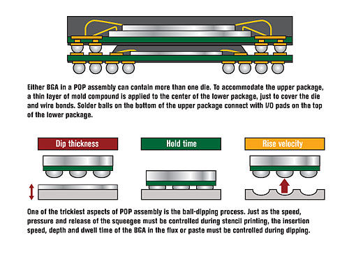
A POP assembly consists of two or more fine-pitch ball grid arrays (BGAs) stacked one atop another. The BGAs range in size from 11 by 11 millimeters to 16 by 16 millimeters. In a two-piece assembly, the bottom package is usually a high-density logic device, while the top package is a high-capacity memory device. Both devices can contain more than one die. To accommodate the upper package, a thin layer of mold compound is applied to the center of the lower package, just to cover the die and wire bonds. Solder balls on the bottom of the upper package connect with I/O pads on the top of the lower package. The finish on the pads can be nickel-gold or copper organic solder preservative.
The solder balls on the upper package are 0.4 millimeter in diameter with a pitch of 0.65 millimeter. The solder balls on the lower package are 0.3 millimeter in diameter with a pitch of 0.5 millimeter. (In the near future, the balls on the upper package could be spaced as little as 0.5 millimeter apart, while the balls on the lower package could be spaced just 0.4 millimeter apart.) All totaled, a two-BGA POP assembly can be 1.2 to 1.6 millimeters tall.
POP assemblies are produced using the standard surface-mount process-with an extra hitch. The BGAs are fed from tape or trays. First, solder paste for the lower BGA is deposited on the board with a stencil printer, and the BGA is placed onto the board. Next, the second BGA is picked up and-here’s the hitch-dipped into a film of specially formulated “tacky” flux or solder paste just far enough to wet the balls. The second BGA is then placed atop the first one, and the entire board is reflowed as normal, preferably in a convection oven with a nitrogen atmosphere.
An underfill material can be applied to one or both BGA interfaces after reflow, though industry experts disagree over whether the extra step is necessary. To meet drop-test requirements for handheld electronic devices, BGA manufacturer Amkor Technology (Chandler, AZ) recommends an underfill for lead-free BGAs with nickel-gold pads. However, some evidence also suggests that an underfill could cause BGA connections to fail thermal cycling tests, so further research is under way.
In some cases, existing pick-and-place machines can be retrofit to accommodate the POP process. The key is accuracy, says Richard Boulanger, vice president for advanced semiconductor assembly at Universal Instruments Corp. (Binghamton, NY). To avoid tolerance stack-up issues, placement machines for POP assembly must be more accurate than machines that place components in a single layer. If the first BGA is off by a few microns in one direction, and the second BGA is off by a few microns in the opposite direction, they may not make an electrical connection. Compounding the problem is that lead-free solder is not as self-correcting during reflow as tin-lead solder.
As a result, solder balls should be 75 percent to 90 percent on target with their pads, Boulanger says.
Components Take a Dip
Other than placement, the trickiest part of POP assembly is the ball-dipping process. For high yields, it must be consistent. Similar amounts of flux or paste must adhere to each ball. If there’s too little flux or paste on the balls, the assembly could have opens or insufficient solder joints. If too much material sticks to the balls, it could cause bridging.Just as the speed, pressure and release of the squeegee must be controlled during stencil printing, the insertion speed, depth and dwell time of the BGA in the flux or paste must be controlled during dipping. And, just as the rheology and composition of the solder paste are critical for good printing, so too are the rheology and composition of the flux or paste for good dipping. Before dipping, the material should be spread in a thin, uniform film that is free of bubbles.
For best results, the balls should be dipped to a depth of 50 percent to 66 percent of their height, and the BGA should be held in the material for 0.1 to 1 second, says Michael Liberatore, Ph.D., director of R&D at Cookson Electronics (Providence, RI). The insertion and removal speed will vary, depending on the rheological properties of the flux or paste.
Suppliers of electronics assembly machines are answering this challenge. For example, Siemens Electronics Assembly (Norcross, GA) has introduced a linear dipping unit for its SiPlace X-Series placement machines. The unit can spread a film of flux 50 to 400 microns thick with an accuracy of ±5 microns. The unit has a reservoir that can be equipped with an automatic refill device, so the placement machine can operate without interruption. The viscosity of the flux can range from 2,500 to 150,000 centipoise.
Flux and paste suppliers are also on the job. Tacky flux is a water-soluble, no-clean formulation containing a mild- to medium-active organic acid. When formulating tacky flux, suppliers must balance viscosity and elasticity so the material can be spread in a flat, even film for dipping, says Liberatore. If the material is too thick, the film will have streaks or voids. If it’s too thin, the film won’t hold its shape or maintain an even thickness over time. Similarly, the flux must be thick enough to adhere to the solder balls without being so thick that it strings when the component is withdrawn from the film.
Recently, suppliers have added new properties to tacky flux. For example, Henkel Corp. (Irvine, CA) has introduced a new material, called Hysol FF6000 epoxy flux, that combines the functions of a tacky flux and an underfill. The flux provides the action necessary for solder joint formation, and the epoxy encapsulates each solder sphere for added support and protection. Combining the underfill with the flux eliminates the need to dispense and cure a separate underfill later.
Henkel has also introduced a tacky flux that will help ensure that every ball on the upper BGA has an adequate amount of flux after dipping.
“The problem with dipping the BGA into the flux is knowing whether the flux has been applied to the entire component,” says Mark Currie, Ph.D., global product manager for semiconductor soldering at Henkel. “Our new flux has a blue dye that’s visible to an upward-looking camera.”
Like tacky flux, solder paste for dipping has different rheological properties than paste for standard surface mount assembly. “The paste will be lower in viscosity than you are used to for printing or even dispensing,” says Jim Hisert, applications engineer with Indium Corp. (Utica, NY). “You can actually pour the paste out of the jar into a flux reservoir.”
Pastes with 75 percent to 80 percent metal content and Type IV particles (20 to 38 microns in diameter) work best for dipping, adds Brian Toleno, Ph.D., applications engineering team leader for Henkel. Pastes with higher metal content have too much tack force for consistent application during dipping, while those with larger particles tend to produce bridging during reflow.

Henkel
has introduced a new material, called epoxy flux, that combines the functions
of a tacky flux and an underfill. The flux provides the action necessary for
solder joint formation, and the epoxy encapsulates each solder sphere for added
support and protection. Photo courtesy Henkel Corp.
Warp Drive
Aside from dipping-related problems, the other major concern in POP assembly is warpage. This can occur in one or both of the BGAs before, during and after reflow. Warpage is caused by mismatches in the coefficients of thermal expansion (CTE) of the die, molding compound and substrate. The lower BGA is particularly prone to warping, because it has a thinner cap of molding compound. Significant warpage can cause opens between the lower BGA and the board, as well as between the BGAs themselves.According to research by Amkor, warpage depends on the size of the die; the thickness and properties of the molding compound; the thickness of the substrate; and the material for attaching the die to the substrate.
To minimize warpage, the die should be as small as possible. A die 8.9 millimeters wide will warp three times as much as a die 6.35 millimeters wide. Increasing the thickness of the molding compound also limits warpage. In one test, Amkor found that increasing the thickness of the compound by just 0.08 millimeter reduced warpage by 35 percent at room temperature. Ideally, the molding compound should have a high CTE, while the die attach adhesive should have a low modulus of elasticity.
Here, too, suppliers are answering the challenge. For example, Henkel recently introduced an epoxy molding compound, Hysol GR9810-1P, that has been specifically formulated for POP assembly. By varying the base resin chemistry, the properties of the material can be tuned to match the package geometry and thereby minimize warping. The compound exhibits long spiral flow and has a good room-temperature working life. It’s also a “green” material, since it does not contain flame retardants.
Warpage can also be controlled by minimizing temperature differentials at each stage of reflow, adds Liberatore. Steep heating gradients should be minimized, and assemblers should not exceed temperature increases of more than 2 C per second.
However, because a certain amount of warpage is inevitable, some experts advocate using solder paste over flux as the medium for attaching the upper BGA to the lower one. “Even with significant warpage, the additional molten solder can act as a metallic bridge between the ball and the pad,” says Liberatore. “Flux cannot.”
Looking for a reprint of this article?
From high-res PDFs to custom plaques, order your copy today!