Assembling Wearable Electronics
With the exception of a few critical steps, assembling circuit boards for wearable electronics is no different than assembling conventional circuitry.
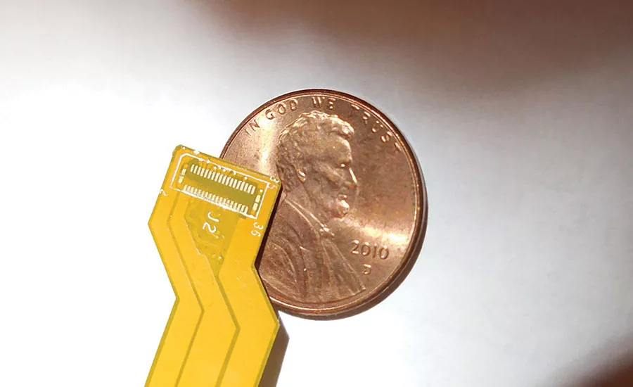
Wearable PCBs come in a variety of odd shapes to suit an application. Photo courtesy NexLogic Technologies Inc.
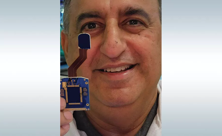
Wearables can contain a combination of rigid and flex circuitry or flex circuitry alone. Photo courtesy NexLogic Technologies Inc.
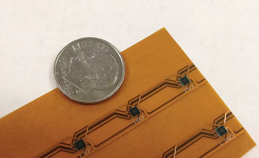
Micro BGAs are attached to a flex circuit for a medical electronics application. These tiny components can house complex circuitry, such as system-on-a chip technology. Photo courtesy NexLogic Technologies Inc.
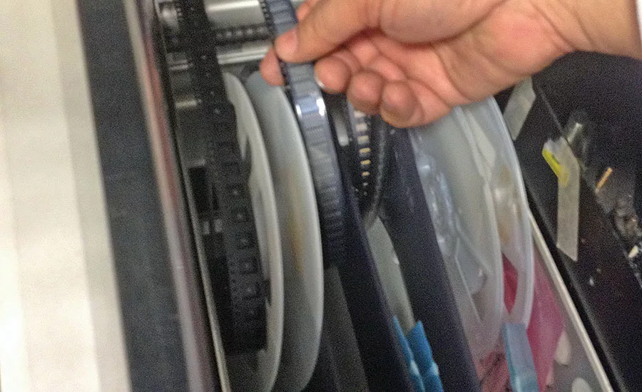
Wearable PCBs can be assembled with standard pick-and-place equipment, but special fixturing is required. Photo courtesy NexLogic Technologies Inc.
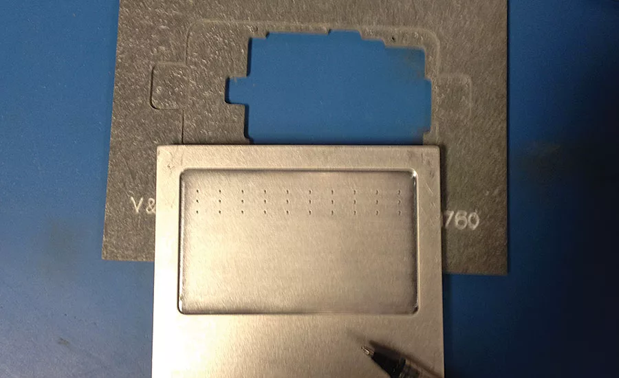
This photo shows the difference between fixtures for conventional PCBs and flexible ones. Photo courtesy NexLogic Technologies Inc.
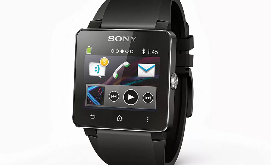
Smart watches and fitness bracelets have helped usher in a new era of wearable electronic devices. Photos courtesy Sony Corp.
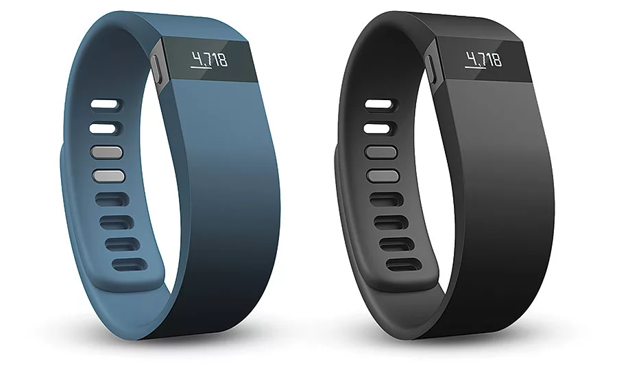
Smart watches and fitness bracelets have helped usher in a new era of wearable electronic devices. Photos courtesy Fitbit Inc.
Wearable electronics initially trickled into the market with Dick Tracy-inspired watches and healthcare bracelets. They quickly gained momentum, however, and it wasn’t long before the wearables market exploded.
Today’s wearables—and new products still on drawing boards—are well beyond the current rage of smart watches. They are rapidly moving into everyday use in medical, fitness, consumer and industrial applications. They will likely soon be adopted for military and aerospace applications, as well.
The same basic technologies used in conventional printed circuit boards (PCBs) are still in play with wearable PCBs. Only this time, all the electronic devices, as well as the PCB itself, are considerably smaller.
Assembly methods for conventional PCBs have been perfected over the course of many years. Processes are stable. Reflow profiles are well-defined and understood. There’s no magic associated with those practices.
However, wearable PCBs are a different animal. They are small and oddly shaped, and the “boards” are made out of flexible materials, such as Mylar or Kapton. To make matters worse, the components mounted to these boards are the smallest available. As a result, these boards demand extra attention on the assembly line.
Wearable PCBs may contain “game-changing” technology, but the processes for assembling them are based on conventional practices. Savvy electronics manufacturing services providers should be able to apply their experience with conventional PCB assembly to building wearable PCBs.
Wearables Overview
Conventional rigid PCBs come in many shapes and sizes, though most are square or rectangular. Board thickness varies from 31 to 93 mils thick and even thicker. Wearable PCBs, on the other hand, come in a variety of odd shapes to suit an application. They are considerably smaller, with sizes ranging from a quarter to a dime or even a shirt button.
Wearables can contain a combination of rigid and flex circuitry or flex circuitry alone. The circuits for most wearables consist of two to four layers of flexible polyester or polyimide. However, the circuitry for newer wearable applications is expected to have 12 to 14 flexible layers of various materials.
Attaching flex circuits to a rigid board calls for a special process. Because rigid and flex circuits have different coefficients of thermal expansion, heat-curing adhesives are used to join them.
Pull testing of soldered components is rarely done with conventional rigid PCBs, but it is often done on flexible circuits for wearable electronics. Such testing is performed to ensure that soldered joints on flex circuits are strong enough to withstand a designated number of bending cycles.
Sensors and Packaging
Sensors are rarely used in conventional PCBs, but they are an increasingly popular feature in wearable electronics. Such sensors are used to measure things like heart rate, blood pressure, and distance traveled. According to market research firm IDTechEx, 3 billion wearable sensors will be in use by 2025, including chemical, stretch, pressure, optical, biopotential and inertial measurement sensors. More than 30 percent of wearable sensors on the market in 2025 will be newly introduced technologies.
A critical part of the assembly process for wearable flex circuits is to test these sensors to their maximum limits. It’s also important to create sufficient soldering pads so that the sensor sits flat on the flex circuit and can contact the skin to collect data.
Electronic device packaging for wearable PCBs also requires careful scrutiny. Just as with conventional PCBs, wearable PCBs continue to shrink. OEMs demand higher performance in ever smaller form factors.
As a result, chipmakers are packing more electronics in smaller pieces of silicon to create such products as systems on a chip (SOC), micro ball-grid arrays (BGAs), chip-scale packages (CSP), and quad flat no-lead packages (QFN).
Tiny components such as 0201s and 01005s are a major concern when assembling any type of PCB, rigid or flexible, simply because they are so small and difficult to process. The 01005 package, used for such passive devices as capacitors, resistors and inductors, is difficult to see with the human eye.
These tiny parts are less of a concern with large, conventional PCBs, since there’s ample real estate for proper printing. Conventional boards also have good-sized pads to create strong, sturdy joints. With wearable PCBs, it’s
another story.
Small pad sizes on a wearable flex circuit may not provide sufficient bonding strength for the components. To ensure adequate bonding strength, the following factors are critical:
-
Direction of the bend of the circuitry.
-
Degree of bend.
-
Number of fold cycles.
-
Application types of the device.
Flex circuits are designed to bend and twist, creating tensions in the solder joint. If assembly isn’t performed correctly, solder joints may crack and components may dislodge.
Now that we know the challenges involved in assembling flex circuits for wearable electronics, I’ll take you through each step of the assembly process.
Stencil Printing
Stencil design and printing are the most important aspects of assembling any type of PCB, since they control how solder paste is deposited on the PCB to create electrical connections. A poorly designed stencil will deposit too much or too little solder paste, resulting in solder defects, such as shorts and opens. Considerably more attention must be paid to stencil design and printing for wearable PCBs. That’s because flex circuits have non-planar surfaces and tiny pads on which solder paste must be homogeneously deposited.
There are three main criteria for stencil design.
First, the stencil should be completely flat, with even surface tension, because it must evenly distribute the paste on all sides of the PCB. This might mean that you will have to work with smaller stencils. The stencil must provide optimum process stability.
Second, the stencil must control solder paste spillage. If solder paste gets spilled over to the next pad (or ball in case of BGAs), the likelihood of creating a short increases. To avoid spillage, the aperture openings must be created with utmost accuracy.
Finally, a good stencil design should incorporate techniques, such as “window paning,” overprinting and underprinting, to match the parts to be soldered. For example, analog packages with heavy ground pins require more solder paste while digital devices need minimal amounts of paste.
Board design can help, too. When designing a wearable PCB, engineers must be extremely precise in defining the surface mount pads. Making the pads a little too small or too big can lead to uneven distribution of solder paste. This includes defining the outlines and where a pad starts and finishes. Pad definition cannot be off by even 5 or 10 percent. Given the tight spacing and overall lack of real estate on wearable PCBs, if pad definition is off by 10 percent, it can lead to a lot of printing headaches.
Pick and Place
Conventional surface-mount PCBs are assembled with high-speed, automatic pick-and-place machines. Components are fed from tubes, trays or reels.
Wearable PCBs are assembled in nearly the same way. The major difference is that wearable PCBs are much more flexible than conventional rigid boards. To ensure accurate placement of components, the surface of the flex circuit—and especially the surface-mount pads—must be extremely stable, straight and precisely positioned.
Fixtures and special tooling help ensure pad stability and precise location of wearable PCBs during pick-and-place operations. These fixtures are custom-made to match the size and shape of the flex. Some fixtures, like those for rigid-flex combo boards, can be quite intricate.
Each fixture must completely enclose the circuitry so that it’s co-planar or flat. This includes the periphery as well as the base line.
Inexperienced contract manufacturers
can misjudge the tooling requirements. They often create aluminum tooling that absorbs most of the heat from a reflow oven. As a result, not enough heat penetrates through the fixture to the flex circuits to create sturdy solder joints.
Cages and Shields
Cages and shields are often used in wearable PCBs and are installed during the pick-and-place operation. Solid or perforated flex shield planes are used to reduce electrical noise and control impedance of signal lines. At times, these cages operate as heat sinks; other times, they are used to block undesired signals in wearable PCBs designed for radio-frequency transmission and reception of signals. During the pick and place operation, these cages must be delicately inserted into the flex circuitry.
Shields come in different sizes, shapes and materials. The shields for wearable PCBs are different than those for conventional rigid PCBs.
Thermal Profile for Reflow
Creating a perfect thermal profile for a wearable PCB undergoing reflow is a challenge. Because wearable PCBs are smaller, they have much less thermal mass than conventional, rigid PCBs. In addition, wearable PCBs often have different thicknesses, as when stiffeners are used, for example.
Conventional circuitry has various amounts of copper and prepreg in the middle of the board. These materials absorb varying amounts of heat. Flex circuits don’t have that, so their thermal profiles will greatly differ.
Fortunately, there are steps that engineers can take to ensure a perfect thermal profile for wearable PCBs. First, the temperature settings in a conduction oven must be lowered to avoid damaging the small boards and the components on them. Special profiling care must be given to temperature settings for lead-free wearable PCBs. The best way is to obtain data from a profiler and adjust accordingly. A profiler may also be necessary to develop the reflow profile for boards with standard, lead-containing solder alloys.
Process engineering experience definitely helps. The process window for wearable PCBs is very tight and needs to be dialed in properly to avoid delamination of boards, burned components or shorts under BGA balls.
Wearable Technology Market to Top $31 Billion by 2020
The overall market for wristwear, eyewear and other wearable electronics is expected to grow at a cumulative annual rate of 17.8 percent over the next five years, reaching nearly $31.3 billion by 2020, according to a new report from market research firm Markets and Markets Inc.
The driving factors for the growth of this market include consumer preference for sophisticated gadgets, increasing popularity of smart watches and wrist bands in the consumer market, increasing growth prospects of next-generation displays and integrated consumer wearables, increasing popularity of wearable fitness and medical devices, and the growing popularity of the Internet of Things.
In 2014, consumer electronics was the biggest segment in terms of market size. However, industrial applications are growing. This is mainly due to increasing demands for wearable scanners and computing devices in warehouse, logistics and the other operations where efficiency is paramount.
Wearable consumer devices include a host of products that are used in applications such as fitness and sports, entertainment and multimedia, and garments and fashion. Wearable electronic devices find compelling applications in fitness and sports. From smart wristwatches that record heart rates to intelligent bands that track physical activities, wearable technology in the form of fitness-monitoring devices are getting increased attention from health-conscious consumers.
Wrist-wearable products are likely to explode in popularity in the coming years. Many leading companies have already launched smart watches and wrist bands. With major companies, such as Apple and Samsung, foraying into the market, the look and feel of wearables should increase immensely. These devices won’t be just computing devices, but style statements. It is no surprise that sports apparel and fitness brands, such as Nike and Adidas, are also launching fashionable electronic wristwear.
The Americas comprise the largest market share in wearable technology due to several factors. One of the most important factors is technological innovations and advancements, which led to the introduction of new products. The increasing demands from consumers and medical applications have also led to the growth of wearable technology in the Americas. Another factor promoting market growth is the increasing incidence of chronic diseases, such as diabetes.
Major players in the wearable technology market are Adidas, Apple Inc., Fitbit Inc., Garmin Ltd., Google Inc., Jawbone Inc., LG Electronics Inc., Nike Inc., Pebble Technology Corp., Qualcomm Inc., Samsung Electronics Co. Ltd., Sony Corp., and Xiaomi Technology Co. Ltd.
Looking for a reprint of this article?
From high-res PDFs to custom plaques, order your copy today!


