SKC to Build Large Semiconductor-Substrate Plant by 2023
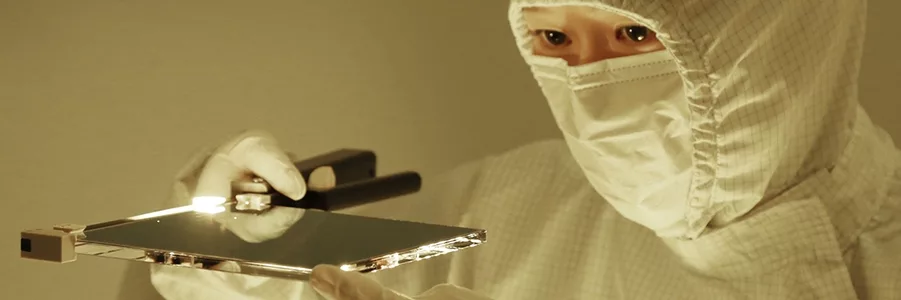
SEOUL—SKC says it will build a 12,000 square-meter plant in Georgia by 2023 to produce a proprietary computing glass substrate for semiconductors. The material will significantly increase the performance and power efficiency of computer chipsets. Production of the substrate will require an investment of $80 million, with technology accounting for $70 million of the total.
According to the company, its unique substrate cuts semiconductor thickness and power consumption in half. SKC also says that it is considering expanding the production capacity to 72,000 square meters per year by 2025, given that the semiconductor packaging market for high-performance computing is rapidly growing due to a surge in data throughput such as AI and data center servers.
In general, semiconductors such as CPU, GPU, and memory are packaged as one component on a substrate together with several multilayer ceramic capacitors before being connected to a PCB. Plastic substrates are widely used, but their uneven surface is problematic for high-performance semiconductor packaging involving repetitive miniaturization.
This method also has low efficiency and limited uses; the package gets thicker due to an interposer, making it hard to be used for mobile applications; The increased distance between the semiconductor chip and the PCB results in larger power consumption, too. In addition, it is difficult to economically produce large-area rectangular substrates required for high performance in round silicon.
These negatives make a glass substrate an attractive solution, according to SKC.
Looking for quick answers on assembly and manufacturing topics? Try Ask ASM, our new smart AI search tool. Ask ASM
Looking for a reprint of this article?
From high-res PDFs to custom plaques, order your copy today!


