Assembly In Action: Semiconductor Platform Assembles Flip Chips
In early 2010, Draper Laboratory was in need of a semiconductor platform that met
two criteria. First, it had to perform flip chip assembly, in which microelectromechanical systems
are connected to circuitry with solder bumps that have been deposited onto the
chip pads. Second, the platform had to be adaptable,
because Draper develops products for a wide range of applications requiring the
latest technology.
 Draper Laboratory of Cambridge, MA, researches and develops products
that solve technology problems faced by its commercial sponsors and various
government agencies. Among the lab’s 1,384 employees are more than 850
engineers, scientists and technicians with expertise in guidance, navigation
and control systems. These systems are used for information integration;
sensors and networks; precision-guided munitions; air traffic flow management;
military logistics; biomedical engineering; and chemical and biological
defense.
Draper Laboratory of Cambridge, MA, researches and develops products
that solve technology problems faced by its commercial sponsors and various
government agencies. Among the lab’s 1,384 employees are more than 850
engineers, scientists and technicians with expertise in guidance, navigation
and control systems. These systems are used for information integration;
sensors and networks; precision-guided munitions; air traffic flow management;
military logistics; biomedical engineering; and chemical and biological
defense.
In early 2010, Draper was in need of a semiconductor platform that met two criteria. First, it had to perform flip chip assembly, or controlled-collapse chip connection, in which microelectromechanical systems are connected to circuitry with solder bumps that have been deposited onto the chip pads. Second, the platform had to be adaptable and state-of-the-art, because Draper develops products for a wide range of applications requiring the latest technology.
Draper eventually purchased the GenesisSC platform, made by Universal Instruments Corp., because it allows complete module assembly through seamless placement of dies and passive components. Draper is now able to assemble flip chips at high speeds, easily transition between products, and create new technologies quickly and cost-effectively. Plus, the platform improves process efficiency and traceability in higher-mix environments.
Justin Medernach, senior member of the Draper technical staff, likes that the platform can place passive components as small as 01005s with an accuracy of ±10 microns.
Another key feature on the GenesisSC is the linear thin-film applicator, which helps Draper meet package-on-package (PoP) requirements. PoP allows discrete logic and memory ball grid array packages to be stacked on top of one another with a standard interface to route signals between them.
Finally, Draper benefits from Universal’s Advanced Process Laboratory (APL), which helps customers develop processes and prototype new products in a full production environment. The APL does this by analyzing technology, process, substrate and component trends. It also leads the Advanced Research in Electronic Assembly Consortia, which cooperates with electronics manufacturers to help them develop new methods and materials.
For more information on semiconductor platforms, call 607-779-5364 or visit www.uic.com.
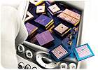
The GenesisSC semiconductor platform allows Draper Laboratory to
assemble flip chips at high speeds. Photo courtesy Universal Instruments Corp.
In early 2010, Draper was in need of a semiconductor platform that met two criteria. First, it had to perform flip chip assembly, or controlled-collapse chip connection, in which microelectromechanical systems are connected to circuitry with solder bumps that have been deposited onto the chip pads. Second, the platform had to be adaptable and state-of-the-art, because Draper develops products for a wide range of applications requiring the latest technology.
Draper eventually purchased the GenesisSC platform, made by Universal Instruments Corp., because it allows complete module assembly through seamless placement of dies and passive components. Draper is now able to assemble flip chips at high speeds, easily transition between products, and create new technologies quickly and cost-effectively. Plus, the platform improves process efficiency and traceability in higher-mix environments.
Justin Medernach, senior member of the Draper technical staff, likes that the platform can place passive components as small as 01005s with an accuracy of ±10 microns.
Another key feature on the GenesisSC is the linear thin-film applicator, which helps Draper meet package-on-package (PoP) requirements. PoP allows discrete logic and memory ball grid array packages to be stacked on top of one another with a standard interface to route signals between them.
Finally, Draper benefits from Universal’s Advanced Process Laboratory (APL), which helps customers develop processes and prototype new products in a full production environment. The APL does this by analyzing technology, process, substrate and component trends. It also leads the Advanced Research in Electronic Assembly Consortia, which cooperates with electronics manufacturers to help them develop new methods and materials.
For more information on semiconductor platforms, call 607-779-5364 or visit www.uic.com.
Looking for a reprint of this article?
From high-res PDFs to custom plaques, order your copy today!


